Microfluidic Device Metrology: AFM, Optical, Confocal Guide
By Priya Deshmukh • 10th May
Microfluidic device metrology and MEMS measurement comparison sound like they belong in a rarefied research lab. They do. But here's what I've learned after years watching precision operations: the same rule applies whether you're checking a turned shaft or verifying a fluidic chip. If operators can't repeat it, it doesn't measure.
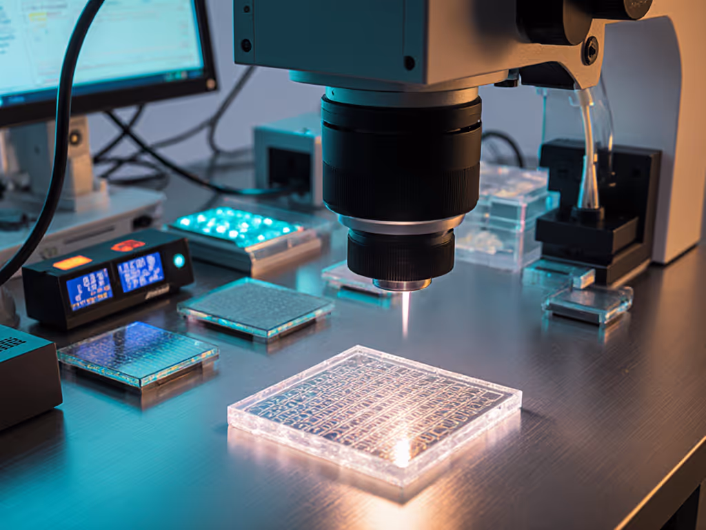
Microfluidic devices (tiny engineered channels that route fluids at microscale) have reshaped diagnostics, drug delivery, and lab-on-a-chip research. But measuring them accurately sits at the intersection of three competing technologies: Atomic Force Microscopy (AFM), optical microscopy, and confocal microscopy. Each one has a role. Each one has a trap. And each one demands that you treat your measurement technique like a repeatable process, not an afterthought.
This guide walks you through how to choose, set up, and execute fluidic chip verification using each method, starting with the principle that repeatability lives in how humans touch tools, not just specs. For a quick primer on accuracy vs precision, see our guide.
Why Microfluidic Metrology Matters Now
Microfluidic devices are used in point-of-care diagnostics, pharmaceutical development, and precision manufacturing. A fluidic channel that drifts 5 microns (invisible to the naked eye) can throw off flow rates, mixing efficiency, and assay accuracy. Customers see failed tests. Regulators see non-compliance.
Quality managers in medical device and pharma sectors face the same pressure I see in precision machining: prove it, trace it, repeat it. The difference is that your measurement tools have to work at scales where a speck of dust is a boulder and operator technique can shift results by 10-20%.
I've seen labs treat metrology as a one-and-done calibration step. Then they're surprised when scan-to-scan variation explodes, or when a new technician's measurements drift from the old one's. The root cause is rarely the instrument. It's almost always how the instrument is being held, positioned, or operated.
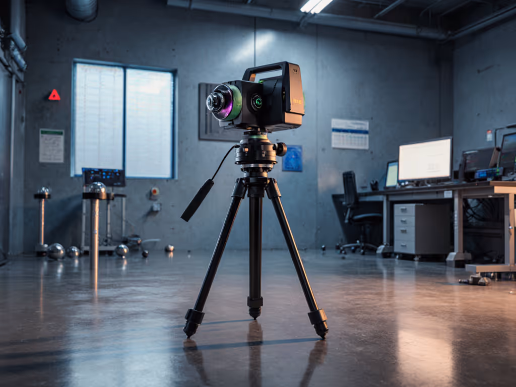
AFM (Atomic Force Microscopy): Ultra-Resolution, High Operator Sensitivity
What AFM Does
Atomic Force Microscopy touches surfaces at nanometer scale using a probe tip. It's the highest-resolution option and indispensable for measuring surface roughness, channel wall geometry, and subtle defects that optical methods miss. If surface finish is your bottleneck, see our surface roughness measurement guide.
Strengths:
- Nanometer-scale lateral and vertical resolution
- True 3D topography of channel walls
- No staining or preparation required for many samples
- Can detect sub-surface features
Weaknesses:
- Slow acquisition (minutes per scan)
- Extremely sensitive to vibration, temperature drift, and humidity
- Steep learning curve; probe force and scanning speed require tuning
- Requires cleanroom or controlled environment
- High capital cost and service overhead
Step-by-Step AFM Measurement Checklist
Before You Start:
- Stabilize the environment. AFM labs must hold temperature to ±0.5 °C and vibration below 0.5 Hz. Check your isolation table. If the building's HVAC cycles or a pump runs nearby, you'll see noise. Relocate or reschedule if necessary.
- Check the probe. Inspect for contamination, tip damage, or residue under low-magnification optical. Document the probe ID and age. Teach-back cue: "A worn probe is like a dull caliper jaw - it'll give you bad data every time."
- Calibrate scanner and tip deflection. Use a calibration sample (grid or grating) to verify x, y, z scaling. Record the calibration constant.
- Set sample temperature. Allow 30 minutes for thermal equilibration.
During Measurement:
- Mount the sample on a clean stage. Use a repeatable fixturing method (vacuum chuck, magnetic plate, or adhesive dot in the same location every time).
- Approach the surface slowly under optical feedback. Stop before contact.
- Set tip oscillation amplitude to 10-20 V (typical). This is critical; too high causes noise, too low causes instability.
- Set scan speed to 0.5-1.0 Hz. Slower is more accurate; faster risks hysteresis.
- Acquire the image in both forward and reverse directions. Compare them for consistency.
- Calculate surface metrics (roughness, channel depth) using the instrument software. Export raw data, not just summary statistics.
- Repeat the same region 2-3 times. Variation should be <5% for height and <10% for derived metrics.
After Measurement:
- Document sample ID, probe ID, date, time, environmental conditions (temp, humidity), and any deviations.
- Archive raw image files and metadata.
- Train it, then trust it: When a new operator takes over, have them repeat a reference scan on a known sample and compare their result to the previous operator's. Teach them how small variations in approach angle or tip force shift the baseline. Use this teach-back to build technique consistency.
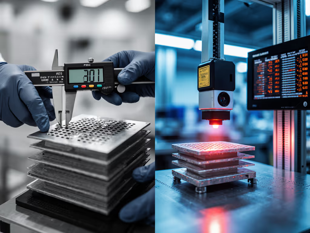
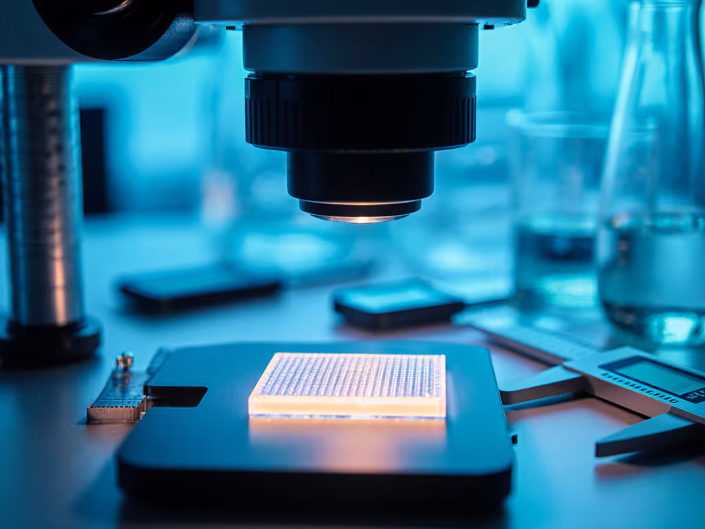
Optical Microscopy: Speed and Simplicity, With Calibration Caveats
What Optical Does
Optical microscopy uses visible light and magnification to image microfluidic channel cross-sections, interfaces, and surface finish. It's fast, familiar, and requires minimal sample prep, but requires meticulous calibration and technique discipline. Common pitfalls here map to measurement error types that quietly inflate scrap and rework.
Strengths:
- Fast (seconds per image)
- Large field of view
- Minimal environmental sensitivity
- Low cost; available in most labs and job shops
- Good for qualitative inspection and defect screening
Weaknesses:
- Diffraction limit (~200 nm lateral resolution)
- Poor depth discrimination; can't reliably measure narrow channel depth
- Software-dependent; pixel-to-micron conversion requires calibration
- Operator bias: lighting angle, focus position, and threshold setting shift measurements
- Not suitable for transparent or semi-transparent channel walls
Step-by-Step Optical Microchannel Measurement Workflow
Setup & Calibration:
- Calibrate magnification using a certified stage micrometer. Place it under the objective at the working height you'll use for samples.
- Capture an image of the micrometer. Using your measurement software, set the pixel-to-micron scale by marking known distances (e.g., 10 micron marks). Record this scale factor.
- Repeat the calibration at different working distances. Optical aberrations mean magnification can shift; create a height-corrected lookup table.
- Set lighting consistently. Use coaxial or ring illumination, not oblique. Document the intensity level (e.g., 50% lamp power).
Measurement Protocol:
- Mount the microfluidic chip on a clean slide. Use the same mounting method every time (e.g., double-sided tape at the same corners, or a clamp fixture).
- Focus on the channel using a coarse focus to find the channel, then fine focus. Document the focal plane.
Related Articles